RM27T0E
_56
Audio / Visual / Telematics
_053721
NAVIGATION / MULTI INFO DISPLAY
_0260991
NAVIGATION SYSTEM(for Navigation Receiver Type)
J
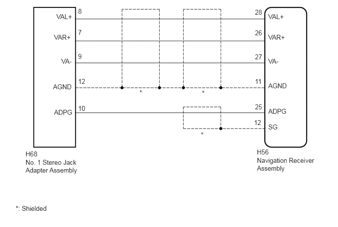
NAVIGATION / MULTI INFO DISPLAY NAVIGATION SYSTEM(for Navigation Receiver Type) Sound Signal Circuit between Navigation Receiver Assembly and Stereo Jack Adapter
DESCRIPTION
The No. 1 stereo jack adapter assembly sends the sound signal from an external device to the navigation receiver assembly via this circuit.
The sound signal that has been sent is amplified by the navigation receiver assembly, and then is sent to the speakers.
If there is an open or short in the circuit, sound cannot be heard from the speakers even if there is no malfunction in the navigation receiver assembly or speakers.
WIRING DIAGRAM
5.688,0.271 6.135,0.438
0.448,0.167
10
false
VAL+
5.406,0.177 5.615,0.344
0.208,0.167
10
false
28
5.688,0.708 6.135,0.875
0.448,0.167
10
false
VAR+
5.406,0.615 5.615,0.781
0.208,0.167
10
false
26
5.688,1.219 6.135,1.385
0.448,0.167
10
false
VA-
5.406,1.125 5.615,1.292
0.208,0.167
10
false
27
5.688,1.74 6.135,1.906
0.448,0.167
10
false
AGND
5.406,1.646 5.615,1.813
0.208,0.167
10
false
11
5.688,2.281 6.135,2.448
0.448,0.167
10
false
ADPG
1.198,0.271 1.573,0.438
0.375,0.167
10
false
VAL+
1.146,0.708 1.563,0.875
0.417,0.167
10
false
VAR+
1.302,1.219 1.573,1.385
0.271,0.167
10
false
VA-
1.125,1.76 1.573,1.927
0.448,0.167
10
false
AGND
1.146,2.302 1.573,2.469
0.427,0.167
10
false
ADPG
5.406,2.188 5.615,2.354
0.208,0.167
10
false
25
1.656,0.156 2.25,0.323
0.594,0.167
10
false
8
1.656,0.604 2.375,0.771
0.719,0.167
10
false
7
1.656,1.115 2.229,1.281
0.573,0.167
10
false
9
1.656,1.646 2.354,1.813
0.698,0.167
10
false
12
1.656,2.219 2.354,2.385
0.698,0.167
10
false
10
0.542,3.188 0.906,3.354
0.365,0.167
10
false
H68
0.542,3.365 1.729,3.781
1.188,0.417
10
false
No. 1 Stereo Jack Adapter Assembly
5.448,3.146 5.854,3.313
0.406,0.167
10
false
H56
5.448,3.323 6.688,3.74
1.24,0.417
10
false
Navigation Receiver Assembly
2.958,1.885 3.573,2.083
0.615,0.198
10
false
*
0.333,4.344 1.854,4.542
1.521,0.198
10
false
*: Shielded
4.281,1.896 4.896,2.094
0.615,0.198
10
false
*
4.26,2.781 4.875,2.979
0.615,0.198
10
false
*
5.688,2.615 6.135,2.781
0.448,0.167
10
false
SG
5.385,2.521 5.594,2.688
0.208,0.167
10
false
12
PROCEDURE
1.CHECK HARNESS AND CONNECTOR (NAVIGATION RECEIVER ASSEMBLY - NO. 1 STEREO JACK ADAPTER ASSEMBLY)
a.
Disconnect the H68 No. 1 stereo jack adapter assembly connector.
b.
Disconnect the H56 navigation receiver assembly connector.
c.
Measure the resistance according to the value(s) in the table below.
- Standard Resistance:
Tester Connection Condition Specified Condition H68-8 (VAL+) - H56-28 (VAL+) Always Below 1 Ω H68-7 (VAR+) - H56-26 (VAR+) Always Below 1 Ω H68-9 (VA-) - H56-27 (VA-) Always Below 1 Ω H68-12 (AGND) - H56-11 (AGND) Always Below 1 Ω H68-10 (ADPG) - H56-25 (ADPG) Always Below 1 Ω H56-12 (SG) - Body ground Always 10 kΩ or higher H68-8 (VAL+) - Body ground Always 10 kΩ or higher H68-7 (VAR+) - Body ground Always 10 kΩ or higher H68-9 (VA-) - Body ground Always 10 kΩ or higher H68-12 (AGND) - Body ground Always 10 kΩ or higher H68-12 (AGND) - Body ground Always 10 kΩ or higher H68-12 (AGND) - Body ground Always 10 kΩ or higher
OK
PROCEED TO NEXT SUSPECTED AREA SHOWN IN PROBLEM SYMPTOMS TABLE
NG
REPAIR OR REPLACE HARNESS OR CONNECTOR