RM27T0E
_56
Audio / Visual / Telematics
_053721
NAVIGATION / MULTI INFO DISPLAY
_0441313
NAVIGATION SYSTEM
J
NAVIGATION / MULTI INFO DISPLAY NAVIGATION SYSTEM Radio Receiver Power Source Circuit
DESCRIPTION
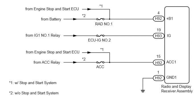
This is the power source circuit to operate the radio and display receiver assembly.
WIRING DIAGRAM
0.927,0.24 2.979,0.417
2.052,0.177
10
false
from Engine Stop and Start ECU
1.5,0.615 2.906,0.927
1.406,0.313
10
false
from Battery
0.938,1.208 2.49,1.469
1.552,0.26
10
false
from IG1 NO.1 Relay
0.948,1.823 3,2
2.052,0.177
10
false
from Engine Stop and Start ECU
5.896,3.083 7.104,3.49
1.208,0.406
10
false
Radio and Display Receiver Assembly
3.479,0.792 4.25,0.979
0.771,0.188
10
false
RAD NO.1
3.219,1.385 4.271,1.635
1.052,0.25
10
false
ECU-IG NO.2
3.521,2.365 4.188,2.656
0.667,0.292
10
false
ACC
5.667,0.594 6.031,0.781
0.365,0.188
10
false
H92
5.667,1.229 6.031,1.417
0.365,0.188
10
false
H93
5.667,2.771 6.031,2.958
0.365,0.188
10
false
H92
6.083,0.594 6.448,0.781
0.365,0.188
10
false
+B1
6.104,1.219 6.469,1.406
0.365,0.188
10
false
IG
6.083,2.188 6.51,2.375
0.427,0.188
10
false
ACC1
6.083,2.75 6.51,2.938
0.427,0.188
10
false
GND1
5.729,1.01 5.938,1.198
0.208,0.188
10
false
19
5.719,1.979 5.927,2.167
0.208,0.188
10
false
15
5.76,0.385 5.906,0.563
0.146,0.177
10
false
4
5.75,2.563 5.896,2.74
0.146,0.177
10
false
1
3.635,0.135 3.844,0.323
0.208,0.188
10
false
*1
3.667,1.729 3.875,1.917
0.208,0.188
10
false
*1
3,0.49 3.208,0.677
0.208,0.188
10
false
*2
3,2.083 3.208,2.271
0.208,0.188
10
false
*2
1.229,2.198 2.302,2.385
1.073,0.188
10
false
from ACC Relay
0.333,2.948 2.385,3.125
2.052,0.177
10
false
*1: w/ Stop and Start System
0.333,3.323 2.385,3.5
2.052,0.177
10
false
*2: w/o Stop and Start System
5.677,2.219 6.042,2.406
0.365,0.188
10
false
H92
CAUTION / NOTICE / HINT
- NOTICE:
-
Inspect the fuses for circuits related to this system before performing the following procedure. (w/o Stop and Start System)
PROCEDURE
1.CHECK HARNESS AND CONNECTOR (RADIO AND DISPLAY RECEIVER ASSEMBLY POWER SOURCE)
a.
0.708,0.938 1.083,1.24
0.375,0.302
2.281,0.948 2.656,1.25
0.375,0.302
1.927,1.813 1.719,0.635
1.719,0.635 1.552,0.635
true
3.063,1.813 2.823,0.51
2.823,0.51 2.656,0.51
true
0.51,2.573 0.344,2.573
0.344,2.573 0.292,2.063
true
3.052,1.948 2.896,2.635
2.896,2.635 2.75,2.635
true
2.354,1.01 2.813,1.208
0.458,0.198
10
false
H92
0.771,0.99 1.229,1.188
0.458,0.198
10
false
H93
2.375,0.438 2.688,0.635
0.313,0.198
10
false
+B1
2.365,2.552 2.813,2.802
0.448,0.25
10
false
ACC1
1.146,0.552 1.594,0.802
0.448,0.25
10
false
GND1
0.563,2.5 1.01,2.75
0.448,0.25
10
false
IG
0.156,0.146 0.604,0.396
0.448,0.25
10
false
*a
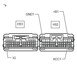
| *a | Front view of wire harness connector
(to Radio and Display Receiver Assembly) |
Disconnect the radio and display receiver assembly connectors.
b.
Measure the resistance according to the value(s) in the table below.
- Standard Resistance:
Tester Connection Condition Specified Condition H92-1 (GND1) - Body ground Always Below 1 Ω
c.
Measure the voltage according to the value(s) in the table below.
- Standard Voltage:
Tester Connection Condition Specified Condition H92-4 (+B1) - H92-1 (GND1) Always 11 to 14 V*1
10.5 to 16 V*2H92-15 (ACC1) - H92-1 (GND1) Ignition switch ACC 11 to 14 V*1
10.5 to 16 V*2H93-19 (IG) - H92-1 (GND1) Ignition switch ON 11 to 14 V
*1: w/o Stop and Start System
*2: w/ Stop and Start System
- Result:
Proceed to OK NG
OK
PROCEED TO NEXT SUSPECTED AREA SHOWN IN PROBLEM SYMPTOMS TABLE
Click hereAudio / Visual / Telematics>NAVIGATION / MULTI INFO DISPLAY>NAVIGATION SYSTEM>PROBLEM SYMPTOMS TABLE
NG
REPAIR OR REPLACE HARNESS OR CONNECTOR