Home › Audio / Visual / Telematics › TELEMATICS › TELEMATICS SYSTEM (for TAS Type) › from 2021.07
RM3700E _56 Audio / Visual / Telematics _093836 TELEMATICS _0483688 TELEMATICS SYSTEM(for TAS Type) J

TELEMATICS  TELEMATICS SYSTEM(for TAS Type)  Telematics Service cannot be Used  


DESCRIPTION

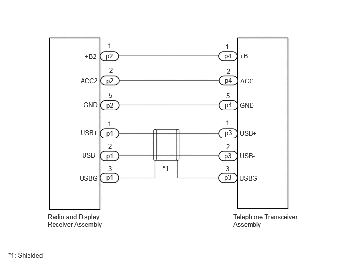
This is the power source and USB circuit to operate the telephone transceiver assembly.

WIRING DIAGRAM
E467940E02
4.948,4.51 6.333,4.927 1.385,0.417 10 false Telephone Transceiver Assembly 1.01,4.51 2.219,4.854 1.208,0.344 10 false Radio and Display Receiver Assembly 0.177,5.333 0.969,5.542 0.792,0.208 10 false *1: Shielded 3.448,3.49 3.719,3.708 0.271,0.219 10 false *1 1.802,1.115 2.167,1.333 0.365,0.219 10 false +B2 5.083,1.104 5.563,1.313 0.479,0.208 10 false +B 1.708,1.625 2.271,1.833 0.563,0.208 10 false ACC2 5.094,1.635 5.656,1.844 0.563,0.208 10 false ACC 1.771,2.135 2.281,2.344 0.51,0.208 10 false GND 5.083,2.146 5.594,2.354 0.51,0.208 10 false GND 1.708,2.729 2.219,2.938 0.51,0.208 10 false USB+ 5.083,2.74 5.594,2.948 0.51,0.208 10 false USB+ 1.74,3.208 2.25,3.417 0.51,0.208 10 false USB- 5.083,3.219 5.594,3.427 0.51,0.208 10 false USB- 1.688,3.698 2.198,3.906 0.51,0.208 10 false USBG 5.073,3.698 5.583,3.906 0.51,0.208 10 false USBG 4.792,2.521 5.052,2.729 0.26,0.208 10 false 1 2.281,2.542 2.542,2.75 0.26,0.208 10 false 1 2.292,3.021 2.552,3.229 0.26,0.208 10 false 2 4.802,3.031 5.063,3.24 0.26,0.208 10 false 2 4.792,3.5 5.052,3.802 0.26,0.302 10 false 3 2.292,3.5 2.521,3.677 0.229,0.177 10 false 3 4.771,2.729 5.281,2.938 0.51,0.208 10 false p3 4.76,3.219 5.271,3.427 0.51,0.208 10 false p3 4.76,3.677 5.271,3.885 0.51,0.208 10 false p3 2.25,3.677 2.76,3.885 0.51,0.208 10 false p1 2.25,3.219 2.76,3.427 0.51,0.208 10 false p1 2.25,2.74 2.76,2.948 0.51,0.208 10 false p1 2.281,0.885 2.542,1.094 0.26,0.208 10 false 1 4.781,0.906 5.042,1.115 0.26,0.208 10 false 1 4.813,1.427 5.073,1.635 0.26,0.208 10 false 2 2.313,1.406 2.531,1.594 0.219,0.188 10 false 2 2.302,1.938 2.563,2.146 0.26,0.208 10 false 5 4.802,1.948 5.063,2.156 0.26,0.208 10 false 5 4.76,1.104 5.271,1.313 0.51,0.208 10 false p4 4.771,1.615 5.281,1.823 0.51,0.208 10 false p4 4.771,2.135 5.281,2.344 0.51,0.208 10 false p4 2.25,2.146 2.625,2.354 0.375,0.208 10 false p2 2.25,1.625 2.594,1.833 0.344,0.208 10 false p2 2.24,1.104 2.583,1.313 0.344,0.208 10 false p2

PROCEDURE

1.CHECK HARNESS AND CONNECTOR (TELEPFONE TRANSCEIVER - RADIO AND DISPLAY RECEIVER ASSEMBLY)
a.

Disconnect the p3 and p4 telephone transceiver assembly connector.

b.

Disconnect the p1 and p2 radio and display receiver assembly connector.


c.

Measure the resistance according to the value(s) in the table below.

Standard Resistance:
Tester Connection Condition Specified Condition

Click Location & Routing(p4,p2,p3,p1)Location & Routing

Click Connector(p4)Instrument Panel>Radio Wiring Sub-Assembly>Telephone Transceiver Assembly for TAS Type

Click Connector(p2)Instrument Panel>Radio Wiring Sub-Assembly>Radio & Display Receiver Assembly

Click Connector(p3)Instrument Panel>Radio Wiring Sub-Assembly>Telephone Transceiver Assembly for TAS Type

Click Connector(p1)Instrument Panel>Radio Wiring Sub-Assembly>Radio & Display Receiver Assembly

p4-1 (+B) - p2-1 (+B2) Always Below 1 Ω
p4-2 (ACC) - p2-2 (ACC2) Always Below 1 Ω
p4-5 (GND) - p2-5 (GND) Always Below 1 Ω
p3-1 (USB+) - p1-1 (USB+) Always Below 1 Ω
p3-2 (USB-) - p1-2 (USB-) Always Below 1 Ω
p3-3 (USBG) - p1-3 (USBG) Always Below 1 Ω
p4-5 (GND) or p2-5 (GND) - Body ground Always 10 kΩ or higher
p3-3 (USBG) or p1-3 (USBG) - Body ground Always 10 kΩ or higher


Result:
Proceed to
OK
NG


OK

2.CHECK HARNESS AND CONNECTOR (RADIO AND DISPLAY RECEIVER ASSEMBLY POWER SOURCE)

NG

REPAIR OR REPLACE HARNESS OR CONNECTOR

2.CHECK HARNESS AND CONNECTOR (RADIO AND DISPLAY RECEIVER ASSEMBLY POWER SOURCE)
a.

Disconnect the telephone transceiver assembly connector.


b.
E407434C04
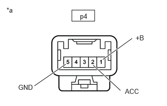
1.479,0.208 1.948,0.438 0.469,0.229 0.708,1.771 1.354,1.323 true 2.479,1.865 1.917,1.344 true 2.719,0.792 2.115,1.229 true 1.646,0.25 2.104,0.448 0.458,0.198 10 false p4 0.135,0.125 0.448,0.323 0.313,0.198 10 false *a 2.792,0.698 3.104,0.896 0.313,0.198 10 false +B 2.573,1.802 3.177,2 0.604,0.198 10 false ACC 0.375,1.719 0.729,1.917 0.354,0.198 10 false GND
*a Front view of wire harness connector
(to Telephone Transceiver Assembly)


Measure the resistance according to the value(s) in the table below.

Standard Resistance:
Tester Connection Condition Specified Condition

Click Location & Routing(p4)Location & Routing

Click Connector(p4)Instrument Panel>Radio Wiring Sub-Assembly>Telephone Transceiver Assembly for TAS Type

p4-5 (GND) - Body ground Always Below 1 Ω


c.

Measure the voltage according to the value(s) in the table below.

Standard Voltage:
Tester Connection Switch Condition Specified Condition

Click Location & Routing(p4)Location & Routing

Click Connector(p4)Instrument Panel>Radio Wiring Sub-Assembly>Telephone Transceiver Assembly for TAS Type

p4-1 (+B) - p4-5 (GND) Ignition switch off 11 to 14 V
p4-2 (ACC) - p4-5 (GND) Ignition switch ACC 11 to 14 V


Result:
Proceed to
OK
NG


OK

NG

REPLACE RADIO AND DISPLAY RECEIVER ASSEMBLY