Home › Audio / Visual / Telematics › AUDIO / VIDEO › AUDIO AND VISUAL SYSTEM
RM27M0U _56 Audio / Visual / Telematics _049135 AUDIO / VIDEO _0234292 AUDIO AND VISUAL SYSTEM J

AUDIO / VIDEO  AUDIO AND VISUAL SYSTEM  Display Signal Circuit between Radio Receiver and Extension Module  


DESCRIPTION

The stereo component tuner assembly sends the sound data signal or image data signal from a device to the radio and display receiver assembly via this circuit.

WIRING DIAGRAM
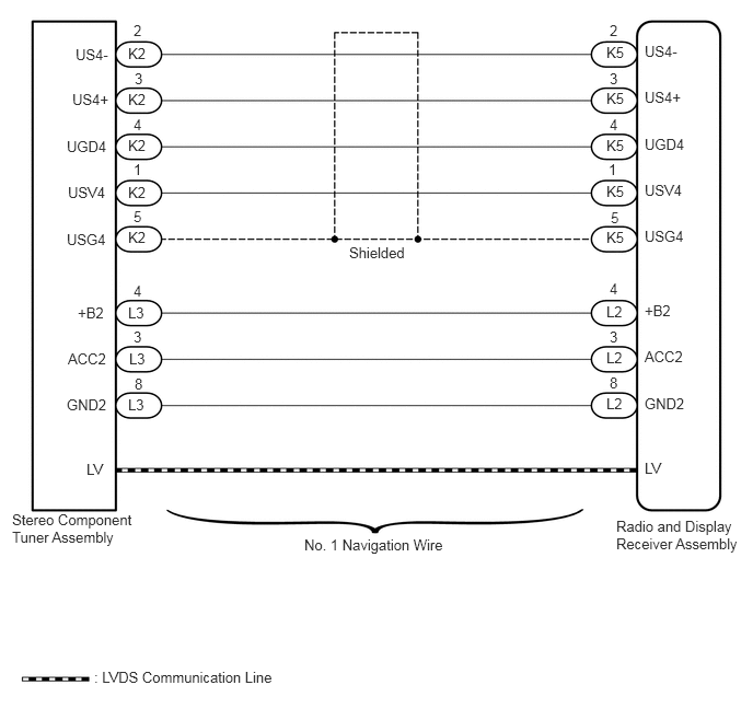
E280906E12
6.135,0.406 6.563,0.583 0.427,0.177 10 false US4- 5.771,0.417 6.198,0.594 0.427,0.177 10 false K5 5.771,0.854 6.198,1.031 0.427,0.177 10 false K5 5.771,1.302 6.198,1.479 0.427,0.177 10 false K5 5.771,1.74 6.198,1.917 0.427,0.177 10 false K5 5.771,2.177 6.198,2.354 0.427,0.177 10 false K5 5.802,0.208 5.927,0.385 0.125,0.177 10 false 2 6.135,0.844 6.563,1.021 0.427,0.177 10 false US4+ 5.802,0.667 5.927,0.844 0.125,0.177 10 false 3 6.135,1.729 6.563,1.906 0.427,0.177 10 false USV4 5.792,1.531 5.917,1.708 0.125,0.177 10 false 1 5.865,4.927 7.083,5.375 1.219,0.448 10 false Radio and Display Receiver Assembly 0.115,4.865 1.302,5.375 1.188,0.51 10 false Stereo Component Tuner Assembly 0.896,6.365 2.802,6.563 1.906,0.198 10 false : LVDS Communication Line 2.896,5.104 4.344,5.313 1.448,0.208 10 false No. 1 Navigation Wire 0.719,0.438 1.073,0.615 0.354,0.177 10 false US4- 0.688,0.865 1.073,1.042 0.385,0.177 10 false US4+ 0.646,1.75 1.031,1.927 0.385,0.177 10 false USV4 6.135,2.167 6.563,2.344 0.427,0.177 10 false USG4 5.813,1.99 5.938,2.167 0.125,0.177 10 false 5 0.635,2.198 1.063,2.375 0.427,0.177 10 false USG4 3.323,2.323 3.969,2.5 0.646,0.177 10 false Shielded 6.135,1.292 6.563,1.469 0.427,0.177 10 false UGD4 0.635,1.313 1.063,1.49 0.427,0.177 10 false UGD4 5.802,1.104 5.927,1.281 0.125,0.177 10 false 4 5.771,2.885 6.198,3.063 0.427,0.177 10 false L2 5.771,3.323 6.198,3.5 0.427,0.177 10 false L2 5.771,3.76 6.198,3.938 0.427,0.177 10 false L2 6.135,3.313 6.573,3.521 0.438,0.208 10 false ACC2 5.802,3.125 5.927,3.302 0.125,0.177 10 false 3 0.646,3.333 1.063,3.51 0.417,0.177 10 false ACC2 6.135,3.76 6.563,3.969 0.427,0.208 10 false GND2 5.802,3.563 5.927,3.74 0.125,0.177 10 false 8 0.635,3.771 1.063,3.948 0.427,0.177 10 false GND2 6.135,2.875 6.563,3.052 0.427,0.177 10 false +B2 0.74,2.896 1.031,3.073 0.292,0.177 10 false +B2 5.802,2.667 5.927,2.844 0.125,0.177 10 false 4 6.135,4.375 6.563,4.552 0.427,0.177 10 false LV 0.823,4.385 1.021,4.563 0.198,0.177 10 false LV 1.219,0.427 1.646,0.604 0.427,0.177 10 false K2 1.219,0.865 1.646,1.042 0.427,0.177 10 false K2 1.219,1.302 1.646,1.479 0.427,0.177 10 false K2 1.219,1.75 1.646,1.927 0.427,0.177 10 false K2 1.219,2.177 1.646,2.354 0.427,0.177 10 false K2 1.271,0.208 1.396,0.385 0.125,0.177 10 false 2 1.281,0.667 1.406,0.844 0.125,0.177 10 false 3 1.271,1.531 1.396,1.708 0.125,0.177 10 false 1 1.271,1.979 1.396,2.156 0.125,0.177 10 false 5 1.271,1.104 1.396,1.281 0.125,0.177 10 false 4 1.219,2.896 1.646,3.073 0.427,0.177 10 false L3 1.229,3.333 1.656,3.51 0.427,0.177 10 false L3 1.219,3.771 1.646,3.948 0.427,0.177 10 false L3 1.271,3.125 1.396,3.302 0.125,0.177 10 false 3 1.281,3.573 1.406,3.75 0.125,0.177 10 false 8 1.271,2.688 1.396,2.865 0.125,0.177 10 false 4

PROCEDURE

1.CHECK HARNESS AND CONNECTOR (RADIO AND DISPLAY RECEIVER ASSEMBLY - SATELLITE RADIO TUNER ASSEMBLY)
a.

Disconnect the K5 and L2 radio and display receiver assembly connectors.


b.

Disconnect the K2 and L3 stereo component tuner assembly connectors.


c.

Measure the resistance according to the value(s) in the table below.

Standard Resistance:
Tester Connection Condition Specified Condition
K5-1 (USV4) - K2-1 (USV4) Always Below 1 Ω
K5-2 (US4-) - K2-2 (US4-) Always Below 1 Ω
K5-3 (US4+) - K2-3 (US4+) Always Below 1 Ω
K5-4 (UGD4) - K2-4 (UGD4) Always Below 1 Ω
K5-5 (USG4) - K2-5 (USG4) Always Below 1 Ω
L2-4 (+B2) - L3-4 (+B2) Always Below 1 Ω
L2-3 (ACC2) - L3-3 (ACC2) Always Below 1 Ω
L2-8 (GND2) - L3-8 (GND2) Always Below 1 Ω
K5-1 (USV4) - Body ground Always 10 kΩ or higher
K5-2 (US4-) - Body ground Always 10 kΩ or higher
K5-3 (US4+) - Body ground Always 10 kΩ or higher
K5-4 (UGD4) - Body ground Always 10 kΩ or higher
K5-5 (USG4) - Body ground Always 10 kΩ or higher
L2-4 (+B2) - Body ground Always 10 kΩ or higher
L2-3 (ACC2) - Body ground Always 10 kΩ or higher
L2-8 (GND2) - Body ground Always 10 kΩ or higher


Result
Result Proceed to
OK A
NG (for Column Shift Type) B
NG (for Floor Shift Type) C


A

2.CHECK NO. 1 NAVIGATION WIRE (LVDS COMMUNICATION LINE)

B

C

2.CHECK NO. 1 NAVIGATION WIRE (LVDS COMMUNICATION LINE)
a.

Replace the No. 1 navigation wire with a known good one.

for Column Shift Type: See page

for Floor Shift Type: See page


b.

Check that the malfunction disappears.

OK.:

Malfunction disappears


OK

END (NO. 1 NAVIGATION WIRE [LVDS COMMUNICATION LINE] IS DEFECTIVE)

NG

PROCEED TO NEXT SUSPECTED AREA SHOWN IN PROBLEM SYMPTOMS TABLE