| Last Modified: 11-27-2007 | 1.6 J | |
| Service Category: Audio/Visual/Telematics | Section: Navigation/Multi Info Display | |
| Model Year: 2008 | Model: LX570 | Doc ID: RM000002TSM003X |
| Title: NAVIGATION / MULTI INFO DISPLAY: NAVIGATION SYSTEM: WIRING DIAGRAM (2008 LX570) | ||
|
Display and Navigation Assembly Communication Error |
WIRING DIAGRAM
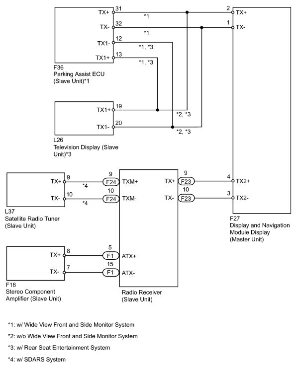
INSPECTION PROCEDURE
PROCEDURE
|
1. |
IDENTIFY COMPONENT SHOWN BY SUB-CODE |
|
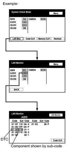
(a) Enter the diagnostic mode. |
(b) Press the "LAN Mon" switch to change to "LAN Monitor" mode.
(c) Identify the component shown by the sub-code.
HINT:
- "118 (display and navigation module display)" is the component shown by the sub-code in the example shown in the illustration.
- The sub-code will be indicated by its physical address.
-
For the component list, refer to Diagnosis Display Detailed Description in the System Description
 .
.
|

|
2. |
CHECK POWER SOURCE CIRCUIT OF COMPONENT SHOWN BY SUB-CODE |
(a) Inspect the power source circuit of the component shown by the sub-code.
Component Table
|
Component |
Proceed to |
|---|---|
|
Radio receiver (190) |
Radio receiver power source circuit
|
|
Stereo component amplifier (440) |
Stereo component amplifier power source circuit
|
|
Parking assist ECU (1AC) |
Parking assist ECU power source circuit
|
|
Satellite radio tuner (1F1) |
Satellite radio tuner power source circuit
|
|
Television display (1F6) |
Television display power source circuit
|
If the power source circuit is operating normally, proceed to the next step.
|
|
3. |
INSPECT RADIO RECEIVER ASSEMBLY |
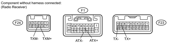
(a) Disconnect the F1, F23 and F24 receiver connectors.
(b) Measure the resistance according to the value(s) in the table below.
Standard Resistance:
|
Tester Connection |
Condition |
Specified Condition |
|---|---|---|
|
F1-5 (ATX+) - F1-15 (ATX-) |
Always |
60 to 80 Ω |
|
F23-9 (TX+) - F23-10 (TX-) |
Always |
60 to 80 Ω |
|
F24-9 (TXM+) - F24-10 (TXM-) |
Always |
60 to 80 Ω |
|
|
4. |
CHECK HARNESS AND CONNECTOR (DISPLAY AND NAVIGATION MODULE DISPLAY - COMPONENT SHOWN BY SUB CODE) |
HINT:
- Start the check from the circuit that is near the component shown by the sub-code first.
-
For details of the connectors, refer to Terminals of ECU
.
(a) Referring to the AVC-LAN wiring diagram, check the AVC-LAN circuit between the display and navigation module display and the component shown by the sub-code.
(1) Disconnect all connectors between the display and navigation module display and the component shown by sub-code.
(2) Check for an open or short in the AVC-LAN circuit between the display and navigation module display and the component shown by the sub-code.
OK:
There is no open or short circuit.
|
|
5. |
REPLACE COMPONENT SHOWN BY SUB-CODE |
(a) Replace the component shown by the sub-code with a normal one and check if the same problem occurs again.
OK:
Same problem does not occur.
|

|

|